A General Guide to DRSSTC Design
Or perhaps better yet, "An Attempt at a General Guide to DRSSTC Design"
Steve Ward, September 2005.
A note to the reader: Within this page I hope to give experimenters, interested in constructing a DRSSTC, some sort of guidance as to how to go about designing and building their DRSSTC. I should make 2 things very clear: 1) designing and building a DRSSTC is NOT a trivial task. It helps to have some experience with power electronic design... if you don't have any experience there, you will get quite a bit of experience when tackling a project such as this! 2) even I am somewhat uncertain as to what the best design is, and as to what operating parameters are best. I will try to discuss these uncertainties, but really the goal of this page is to look at the more mundane aspects of DRSSTC design, basically its construction and component selection. From there the experimenter has the foundation to carry out his own experiments and contribute to this new field of Tesla coil research! The actual operation theory will not be covered in any great detail, and will only enter when necessary. It is up to the reader to have some understanding of logic circuits, inverter basics, and of course, Tesla coil theory.
As with anything I write on my site, please take the information objectively. If there seems to be an obvious flaw in the logic of what I say here, please draw my attention to it as its most likely an error! The following information basically sums up my perspective of a good design, but keep in mind, there are probably many solutions to this problem.
Also, I welcome emails in regards to DRSSTC design. I ask that I can post relevant parts of these emails on this webpage as it would further develop the content within.
Control electronics:
After nearly 2 years of design and revision, I have ended up with what I feel to be a reliable solution for a DRSSTC controller. This design uses primary current feedback as the basis, but could also work from secondary base-current feedback if so desired. I do not like the idea of using an oscillator to derive the drive signal, and primary feedback is preferred in my opinion, so I will focus mostly on that.
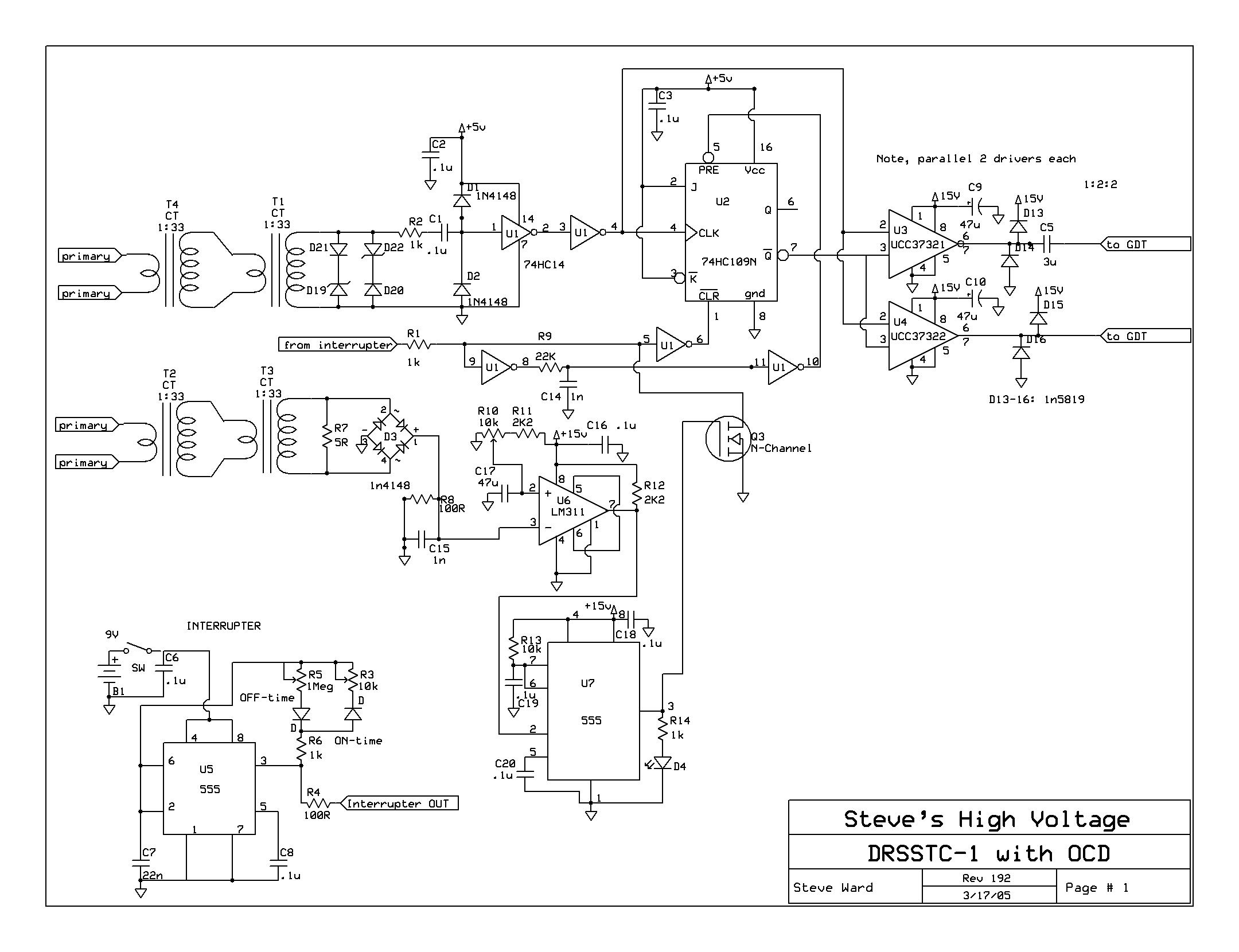
The following is the general schematic for what I currently use in my DRSSTC's:
As seen, it is the control circuit from the DRSSTC-1 project. I use this schematic as an example, some part values may need to be custom tailored to your specific needs... information on that is interspersed within. I think the best way to understand this circuit is for me to explain it, part by part. It may be helpful to print the schematic to follow along. Note that you may need to resize the image for it to fit on a single page.
Power for the electronics is typically provided from a low voltage transformer. Something of around 15VAC at 500mA is suitable. A full-wave rectifier, DC filter cap, and then a 15V and 5V regulator is all that is needed. Be sure to have adequate input and output filtering on the regulators. I typically use a 2200uF capacitor for the un-regulated DC, and then a 1000uF for both the 15v and 5v circuits.
Lets begin by analyzing the fundamental part of this circuit first, that being the feedback loop. In this particular case we use a pair of current transformers (CT's) T4 and T1 in the schematic. Both of them are a 1:33 ratio, and being cascaded, the final current reduction ratio is 1:1089 or roughly 1:1000. The output of T1 is loaded with a pair of zener diodes with ultrafast diodes to block the slow recovery of the zeners (they are not allowed to be forward biased). Since the transformer ratio is ~1:1000, by normal transformer action, the current should be 1/1000th of the primary current, and the voltage should be 1000X greater. But since we have the zener diodes clamping this voltage to 0V and 5 or 15V (depending on your logic level) what we end up with is a clipped sine wave, which approximates a square wave to a high degree. This square wave is then passed through a resistor to limit the current allowable at the input of the logic gate (because the zeners will typically clamp at too high of a voltage). The square wave is also passed through a capacitor to ensure only AC content is passed. To further protect the logic gate of U1, we have a pair of fast logic diodes to clamp any voltage excursions to the supply rails. We then pass our feedback signal through 2 inverter gates on U1. This cleans up our square wave and gives it some hysteresis. Finally our signal is then passed on to the input of the gate drivers as well as the clock input for a flip flop. The flip flop takes signal indirectly from the interrupter and gives an output that is synchronized with the clock input. This ensures that the gate drive shuts down at a feedback transition (indicating a zero crossing of primary current) rather than any arbitrary part of the cycle.
Included in this schematic is a "bare bones" interrupter. I suggest that people start out with this very simple design just to get things working, and then they can progress to more complex interrupter designs that employ multiple oscillators to generate different spark effects. This interrupter could be integrated into the main PC board located with the rest of the electronics, but I prefer a remote interrupter for 2 reasons. 1) its easy to shield the interrupter by putting it in a metal box and using a shielded cable to run the signal to the main board. 2) you can vary the BPS (breaks per second) and ON time in real time to see the effects instantly. Not to mention, you can also control power by varying the ON time.
There are some tricks used to make the JK flip flop (U2) to operate properly in the circuit. As shown when the interrupter goes HI, CLR\ is LOW. This puts Q\ in a HI state. Now, we see that there is a inverter (part of U1) that feeds from the interrupter signal, with its output feeding into an RC circuit and then another inverter. What this does is delay the HI input to the PRE on the flip flop. Note that before the PRE is HI, the output from the flip flop is whatever present on CLR\. If we did not delay the input to PRE, then our interrupter pulse would never be passed along to the gate driver ENABLE (pin 3 on the UCC3732X). Also note that the flip flop only does its synchronized shut down when PRE is high. So this leads to choosing what value we want to use for the RC (R9 and C14). I typically size it so that t=RC=1.5P, where P is the period (in seconds) for 1 RF cycle at the intended operating frequency. Example, the DRSSTC-1 operates near 60khz, so 1 cycle is 16.67uS, so I would want an RC of about 25uS (whereas I use 22uS). The important thing is that PRE does not go LOW before the flip flop does its synchronization. You must allow for at least 1 full cycle of operation after the interrupter has gone LOW for the flip flop to act. To be on the safe side, you could size the RC to be 3*P.
The final feature in this circuit is the active current limiting. Again we I employed a cascaded pair of CTs (1:33 ratio on each). The output is then loaded with a burden resistor. We can calculate the voltage across this resistor related to the input by assuming that the current through the resistor is ~ 1/1000th of the primary current, then its simply I*R=V. We then full-wave rectify this voltage with signal diodes. The output from the rectifiers is then again loaded down with 100 ohms. This 100 ohms is to keep the impedance at the comparator (U6) input low, making it somewhat noise immune. This technique works very well, and without the 100 ohm resistor in place, I find the circuit will falsely trigger on noise. C15 provides extra noise filtering. The LM311 (U6) comparator then compares this feedback voltage with a reference source. This reference voltage must be set experimentally for optimal results, mostly due to the fact that we cant be certain of the voltage that D3 (the full wave rectifier) drops. We can approximate it, though. Assuming a 5 ohm burden, and a desired limit of 1000A, that would be 5V across the burden. The diodes might drop .5V, or 1V drop total, so our output is really 4V. We would then set the comparator reference voltage to about 4V. If you wanted to limit at something lower like 100-200A, then you would have to increase the resistance of the burden resistor to perhaps 10-20 ohms. Note then, that the 100R on the output of the full-wave rectifier would have more of an effect on the final output voltage. So again, it is recommended that this circuit is fine tuned with trial and error. I typically set the limiter too low and watch the primary current on an oscilloscope (using a home made CT). I then operate the coil with free air streamers only if possible. I then set the limiter so that it just barely does not trigger with free air streamers. Then I check that the limiter does engage with ground arcs as it should. So back to the circuit itself... when the voltage at pin 3 exceeds the reference voltage on pin 2 of the comparator, the output of the comparator goes LOW. This negative going edge triggers pin 2 on the 555 timer (U7). The 555 is wired as a mono-stable, the pulse width is set to about 1.1mS. This is sufficiently long to guarantee that it will disable the remainder of the operating period, as well as give a visual indication on the LED (D4). You don't want to make the output pulse so long that it can inhibit the next pulse from the interrupter. The output from the 555 then turns on a small MOSFET which pulls the interrupter signal LOW, shutting down gate drive on the next switching transition. I chose to use a MOSFET here for noise immunity, apparently small bipolar transistors could trigger from noise alone. The MOSFET would need several volts of noise on the gate to turn it on.
Finally we have the gate drivers. These drivers were chosen because 1) they are rugged 9A pk output drivers, and 2) they have an ENABLE function. This is important because the ENABLE, when LOW, forces the drive output LOW (where as an inverting gate driver would go HIGH if you disabled its drive signal). Each gate driver has output protection diodes. The function of these diodes is to clamp any voltage spikes to the supply rails. Be sure to use tantalum or ceramic capacitors across the supply pins of the gate drivers, they need this reservoir of energy to deliver high currents during the switching transitions. C5 is a DC blocking capacitor. It must be large because it forms a voltage divider with the gate capacitance of the IGBTs, so you want the voltage dropped across C5 to be very small. I have never required more than 10uF here, generally 2-5uF is ok for smaller IGBT gates.
IGBT vs. MOSFET:
A question that I often get is "why IGBTs and why not MOSFETs?". The answer is relatively simple, and it deals with the losses in each device. A MOSFET has an ON resistance, so power dissipated in a MOSFET is given by I*I*R. As I increases, the losses go up exponentially. An IGBT on the other hand acts like a diode and has a relatively constant voltage drop, so power dissipated is given by V*I. Losses go up linearly as current increases, and this really makes all the difference when running 100's of amps pulsed. To further exploit the pulse capabilities of the IGBT, we drive the gates to a higher voltage (30V is typical). This lowers the volt drop, and keeps the IGBT in saturation even at extreme conduction currents.
Power electronics:
The best topology by far for DRSSTC work is the half-bridge or full-bridge. The full-bridge offers a higher output voltage for the same input voltage, but at the expense of greater parts count.
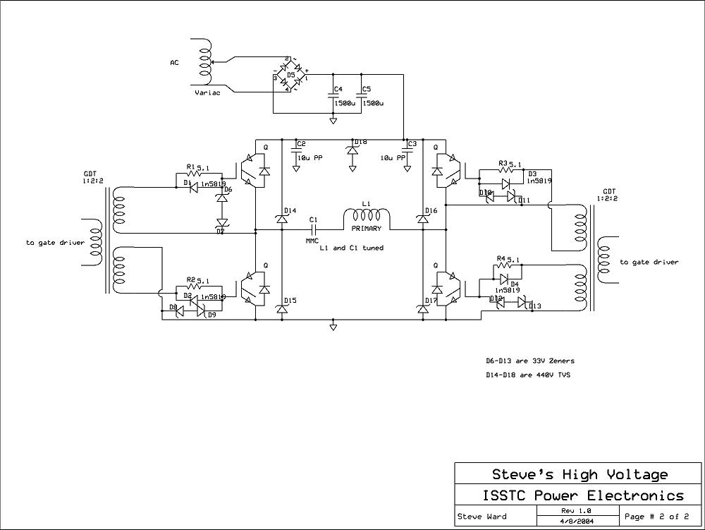
Some tips for constructing your bridge inverter:
Keep all connections as short as possible. When switching high currents quickly, voltage transients will develop (V=-L*dI/dt). So keeping inductance to a minimum is very crucial since we don't want to reduce switching speed (that would impart greater losses as the IGBT would be in its "linear" region for a greater period of time).
Put decoupling capacitors across the power supply rails. These capacitors should have a very minimal inductance to each of the half-bridge sections. This capacitor is to catch any voltage excursions beyond the supply voltage. A majority of the voltage spikes seen across the IGBTs can be absorbed by these capacitors. For smaller coils I have used around 10uF of capacitance here per half-bridge. My larger coil uses 14uF per half-bridge section. Use high quality capacitors with low inductance and high peak and RMS current ratings. I found the general electric 40L and 42L series capacitors to work well. The CDE film caps would also make an excellent choice, though getting a high capacitance might be difficult.
Use Transient Voltage Suppressors (TVS) from collector to emitter of each IGBT. The TVS should typically be the 1.5kW type. I use strings of the 1.5KE220CA seriesing up as many as needed. They are rated to stand off 220V, so for 600V IGBTs I use 2 in series. For my 1200V IGBTs I use 4 in series for 880V clamping. Note that the TVS do not start to clamp "hard" until you exceed their voltage rating by some %, check the spec sheet for the exact breakdown voltage. Keep the TVS physically very close to the IGBT terminals. The TVS are there to catch the very fast transients that the decoupling capacitors may not catch. IGBTs do not tolerate overvoltage very well at all!
Use TVS or zeners on the IGBT gates. If there is a voltage transient across the C-E junction, and the gate has some capacitance with respect to the collector, this transient will appear on the gate as well (its capacitively coupled through). I use 30V TVS of the 600W type. Be sure to get the bi-polar TVS. Since we are driving the gates at their limitations, we need to be extra careful not to damage them, so TVS or zeners go a long way to protect them.
Keep the large filtering capacitors electrically close to the bridge as well. The large electrolytic capacitors serve as an energy resivior supplying hundreds of amps on demand. Too much inductance or resistance in this path will hinder performance. Having the main filter capacitors close to the bridge also reduces the burden on the decoupling capacitors. I typically size these filter capacitors such that they store maybe 20 to 50X the intended "bang" energy. The bang energy is simply given by (input power)/(bangs per second). For example, my DRSSTC-1 uses 880J of storage and runs about a 12J bang (it can really support much more!). Really, I could have used as little as 375J and have done ok (this has been tested) but these capacitors were on hand.
Use heavy conductors. Many of my bridges were made using double sided PC board. The "traces" are maybe 1.5" wide or more, and both sides of the board are paralleled together. This seems to work very well. For those really big bridges, you might resort to using copper buss-bar, but if you are running those power levels, you are probably beyond this article ;-).
Of course, look at my DRSSTC pages for pictures of my work to get ideas for your own layout.
Tank circuit parameters and components:
This is a difficult subject to say the least. Experiments have shown that a shorter burst length (operating the coil for fewer cycles) seems to be more efficient at producing long sparks. The trick is to get enough energy delivered in a short amount of time. On the other hand, we have component limitations. Delivering the energy faster means that we have to achieve higher peak currents. So we look for a balance between ON time and peak currents.
Secondary circuit parameters:
Operating parameters:
...A work in progress...